
Major breakthrough in semiconductor sector
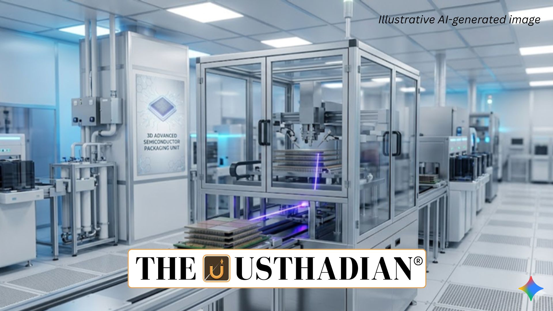
Odisha Hosts India First 3D Semiconductor Packaging Unit: India has taken a significant step in advanced electronics with the foundation of its first 3D semiconductor packaging unit in Info Valley, Odisha. The project involves an investment of around ₹2,000 crore, marking a major push towards high-end chip manufacturing capabilities.
This unit focuses on 3D packaging technology, which enhances chip performance by stacking components vertically. It is crucial for next-generation technologies like AI, 5G, and high-performance computing.
Static GK fact: Odisha’s capital is Bhubaneswar, which is emerging as a major IT and electronics hub in eastern India.
What is 3D semiconductor packaging
Unlike traditional flat chip designs, 3D semiconductor packaging involves stacking multiple layers of circuits. This improves speed, efficiency, and space utilization in electronic devices.
Such advanced packaging is essential for sectors like defense systems, data centers, and smart devices, where compact and powerful chips are required.
Static GK Tip: Semiconductor packaging is the final stage of chip manufacturing, following fabrication and testing.
Strategic importance for India
This project strengthens India’s push for self-reliance in semiconductor technology under national initiatives like India Semiconductor Mission. It reduces dependence on imports and enhances domestic capabilities.
The unit will support critical sectors including defense, telecommunications, and digital infrastructure, making India more resilient to global supply chain disruptions.
Static GK fact: India is one of the fastest-growing electronics markets globally, driven by smartphone and digital expansion.
Economic and regional impact
The project is expected to generate employment and attract further investments into Odisha’s electronics ecosystem. It will also boost ancillary industries like logistics and component manufacturing.
Info Valley is being developed as a dedicated electronics manufacturing cluster, positioning Odisha as a key player in India’s semiconductor landscape.
Static GK Tip: Electronics manufacturing clusters (EMCs) are promoted by the Government of India to boost industrial growth.
Way forward
While this is a major milestone, India still needs to expand into full-scale chip fabrication units (fabs). Continuous investments, skill development, and global collaborations will be essential.
The success of this project can pave the way for more advanced semiconductor technologies in India, strengthening its position in the global tech supply chain.
Static GK fact: Semiconductor fabs require extremely high capital investment and cutting-edge technology.
Static Usthadian Current Affairs Table
Odisha Hosts India First 3D Semiconductor Packaging Unit:
| Topic | Detail |
| Project | 3D Semiconductor Packaging Unit |
| Location | Info Valley, Odisha |
| Investment | ₹2,000 crore |
| Technology | 3D chip packaging |
| Key Sectors | AI, 5G, defense, computing |
| Initiative Support | India Semiconductor Mission |
| Economic Impact | Job creation and industrial growth |
| Strategic Goal | Self-reliance in semiconductor sector |